Wafer layout and alignment marks
A mask set isn't finished when one die looks right. Before tapeout you still need to know how that die steps across a real wafer — how many you get, how many the edge throws away — and you need alignment marks that print in the same place on every level, so a five-mask process actually lands on top of itself under the aligner. This guide covers both: , which step-and-repeats a die cell across a wafer blank with dicing lanes and an edge exclusion, and the alignment-mark pair under Verify — Place alignment marks…, which drops one mark type at a list of coordinates across several layers in a single undo step, and Check mark alignment…, a read-only geometric check that reports whether every level agrees.
- Time: ~25 min
- You'll need: Glyph open on a blank document — if you have been editing something else. Nothing is imported and nothing is pre-supplied: steps 1 to 6 build the die, its two mask layers and their field tones from that blank document, because the wafer and mark tools downstream depend on all of it.
Name the three layers. A blank document starts with three layers,
1/0,2/0and3/0, namedLayer 1,Layer 2andLayer 3. The right-hand panel opens on its Layers tab; double-click a layer's name to turn it into a text box, type the new name and pressEnter. Name1/0Active,2/0Metal1 and3/0Wafer. The name is Glyph's label for your convenience — GDS stores only thelayer/datatypenumber pair beside it, which is why the numbers stay put while the names change.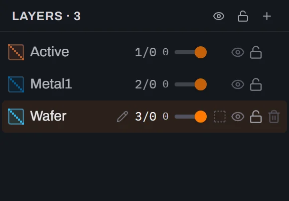
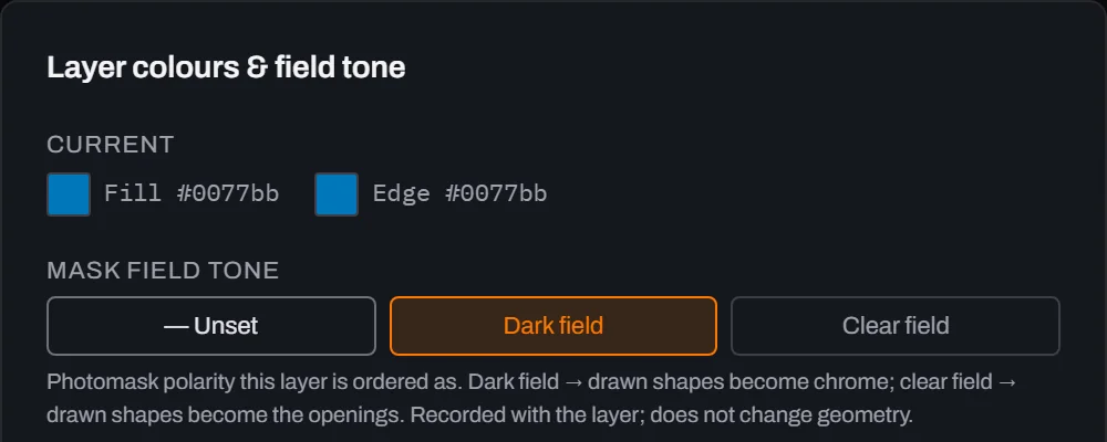
Give Metal1 a dark-field tone. Click the small hatched colour swatch at the left end of the Metal1 row — the leftmost thing on the row, about the size of the text beside it. That opens the Layer colours & field tone dialog. Under MASK FIELD TONE, click Dark field; it lights up in orange as soon as it takes, and the hint underneath states what you just declared: "Dark field → drawn shapes become chrome; clear field → drawn shapes become the openings." Leave Active unset (a layer with no declared tone is treated as clear field). This is load-bearing later: steps 11 and 12 emit a different shape on Metal1 precisely because of this setting.
 View full image
Create the die cell. Click Close in the dialog. Back in the panel, switch to the Cells tab and click the + button at the right of the
CELLSheader, typeDIE, and pressEnter. ADIErow appears belowTOP. Step 2 also left a smallDFbadge on the Metal1 row back in the Layers tab — you'll first see it in step 5's screenshot — and that badge is how you check the tone stuck without reopening the dialog.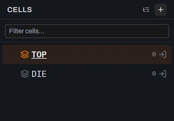
Find the enter-cell icon. Hover the
DIErow and seven small icons appear along its right end. Left to right they are: an eye (hide this cell's instances), a square (show its instances as a box), a pencil (rename), stacked cubes (insert an instance, an SREF), a 3×3 grid (insert an array, an AREF), an arrow pointing into a bracket — that is enter-cell — and a waste bin (delete). The enter arrow is the second from the right, and it is the only one of the seven that stays visible when you are not hovering. Double-clicking anywhere on the row does the same thing.
Enter DIE and draw the 4.4 mm active area. Click that arrow. The breadcrumb at the top-left of the canvas now shows
TOP (top), a chevron, andDIE, and the hint strip along the bottom of the window saysEditing DIE — Esc to go back. Two things before you draw. First, switch back to the Layers tab and click the Active row: the highlighted row is the layer new shapes land on, and after the renaming in step 1 it is still whichever row you touched last — make Active current before drawing. Second, this is the first step where you move around the canvas freely — scroll the mouse wheel to zoom at the pointer, holdSpaceand drag (or drag with the middle mouse button) to pan, and pressCtrl+0for when you have lost the drawing.Now arm the Box tool in the toolbar (the square icon, shortcut
B) and drag out a rough square — you cannot drag an exact 4400 µm, and you don't need to. With the box still selected, type the real numbers into the PROPERTIES panel, which is authoritative: W4400, then H4400, then X300, then Y300. Anchor is on Corner, so X and Y are the box's lower-left corner, and W and H grow the box from that corner — it stays put whichever order you type the four numbers in. The status bar reads1 shape · 1 selected.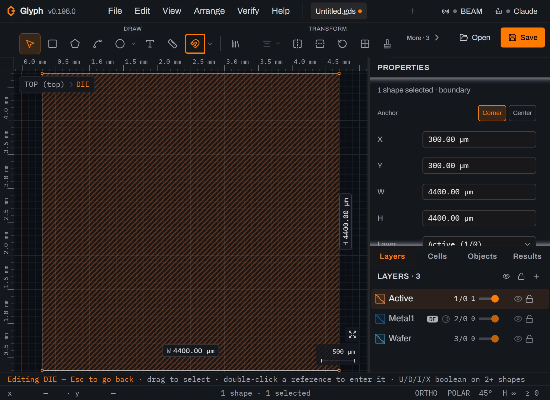 View full image
Draw one metal trace on Metal1. In the Layers tab click the Metal1 row so it becomes the current layer, then arm Box again — Glyph's draw tools are one-shot, so a committed box reverts the tool to Select and a second drag without re-arming would silently marquee-select instead of drawing. Drag a rough sliver inside the active-area square, then set W
1500, H50, X500, Y2350, pressingEnterafter each. The Properties panel's Layer row confirmsMetal1 (2/0), and the status bar reads2 shapes · 1 selected. That 1500 µm length is deliberate: the mark check in step 13 ignores any shape whose bounding box exceeds 500 µm on either axis, so a real die feature is never mistaken for an alignment mark. Your die is done — a 5 mm × 5 mm cell with a 4.4 mm active area (a solid square — "area", not an outline) and one metal trace.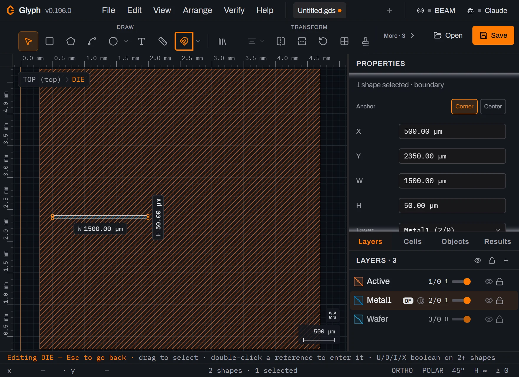 View full image
Open the wafer planner. Click
TOP (top)in the breadcrumb to leave the die, then choose . The dialog opens on the 150mm preset — 150 mm diameter, a 57.5 mm primary flat facing the bottom, the SEMI-standard shape.DIEis the only cell other thanTOP, so the DIE CELL picker defaults to it and Generate is already enabled. First confirm four values every later number depends on: DIE WIDTH and DIE HEIGHT5000, PITCH X and PITCH Y5100(µm). Then change two fields: set OUTLINE LAYER to3/0 — Wafer, so the wafer rim and the dicing lanes land on their own layer instead of on a die layer, and set LANE WIDTH (µm) to100. Note DIE ORIGIN, left onLower-left of footprint: it says where the die cell's own origin sits inside its 5000 µm footprint, so with it on lower-left the die grid starts with a footprint corner at (0, 0) — which is what makes the mark coordinates in step 11 computable. The die fields are in µm, so5000is 5 mm. The stats strip already reads 553 dies as 26 AREFs, 0 SREFs, 231 dropped, computed from the numbers above with no wafer drawn yet.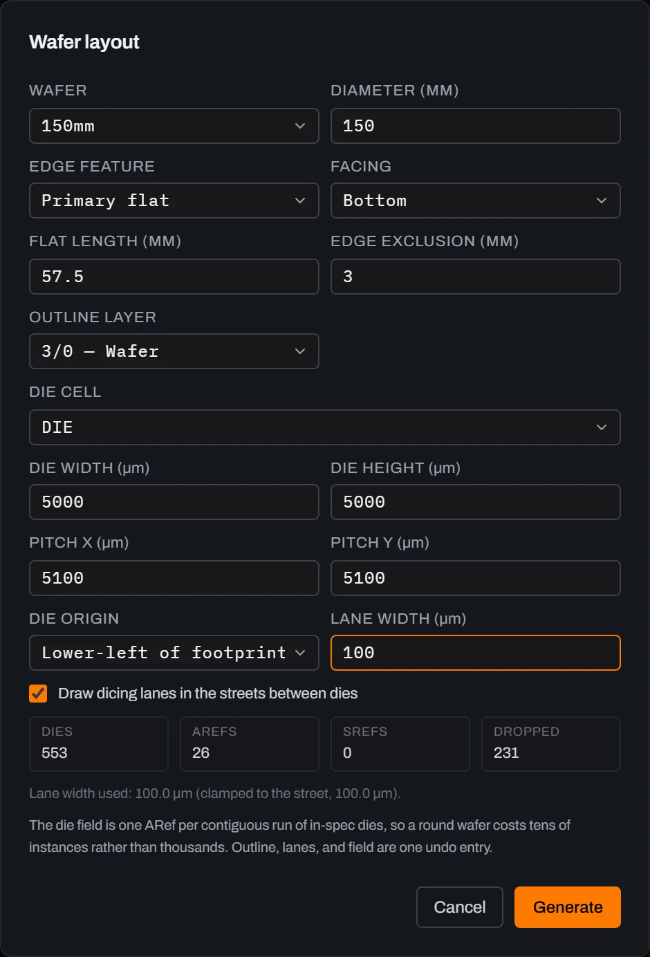 View full image
Watch the preview react. Type
5into EDGE EXCLUSION (MM), replacing the3. The stats strip updates instantly, before you have generated anything: 532 dies, 25 AREFs, 144 dropped — 21 fewer dies for 2 mm more exclusion. This is the whole point of the live preview: you can feel out edge exclusion, pitch, and lane width against the die count before committing a single shape.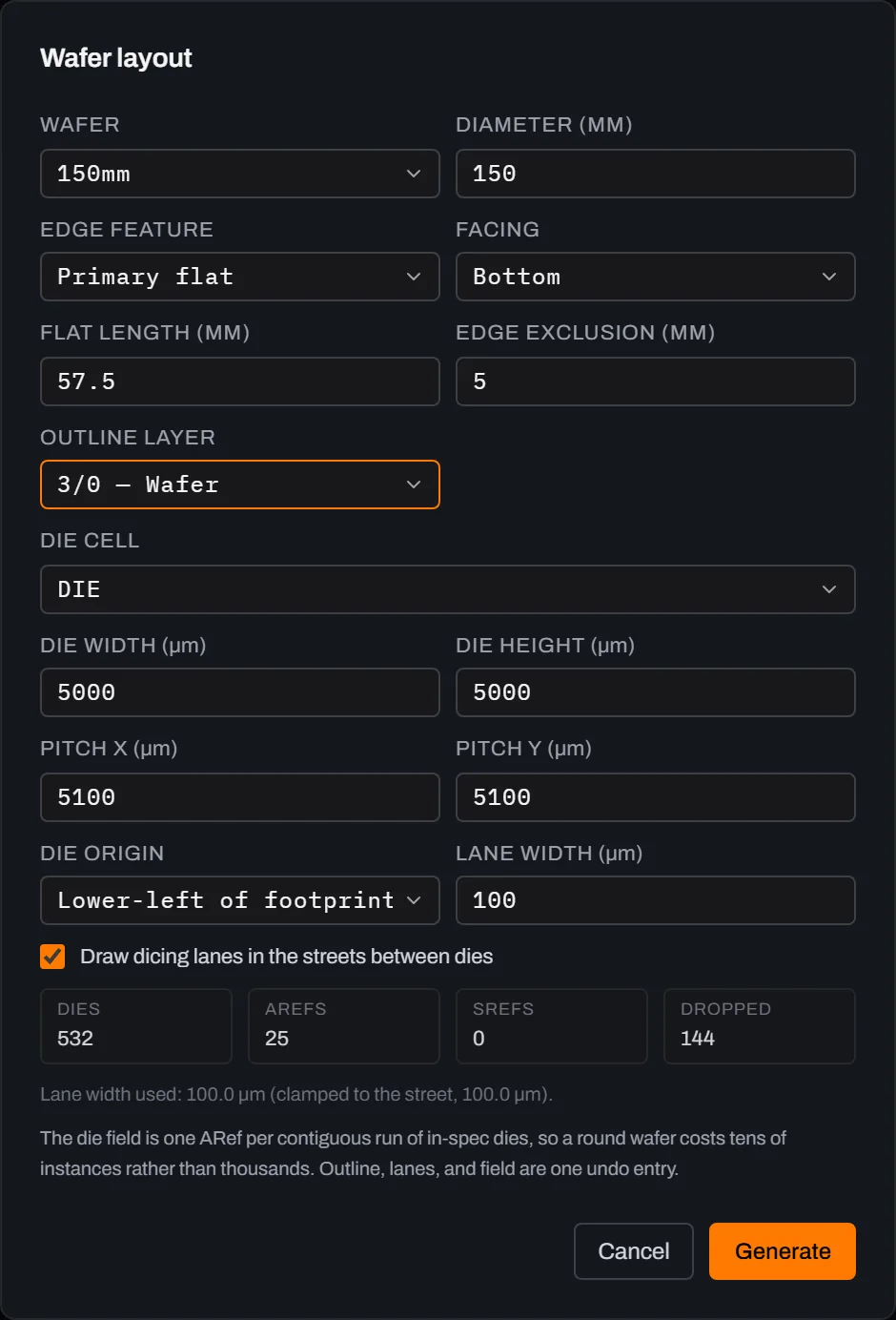 View full image
Generate at 3 mm exclusion. Set edge exclusion back to
3and click Generate. Glyph writes the wafer outline, the dicing lanes, and the die field intoTOPas one undo entry: 58 plain shapes (2 for the outline, 56 lane rectangles) plus 26 AREFs — not 553 SREFs. Each AREF is one row's contiguous run of in-spec dies (cols × 1), because AREF has no sparse form and a round wafer clipped against a rectangular grid isn't one rectangle; a full 150 mm wafer at this pitch still costs only ~26 instances. The toast reads553 dies placed as 26 AREFs + 0 SREFs across 26 rows; 231 grid positions dropped at the edge.and the status bar reads58 shapes · 26 arrays.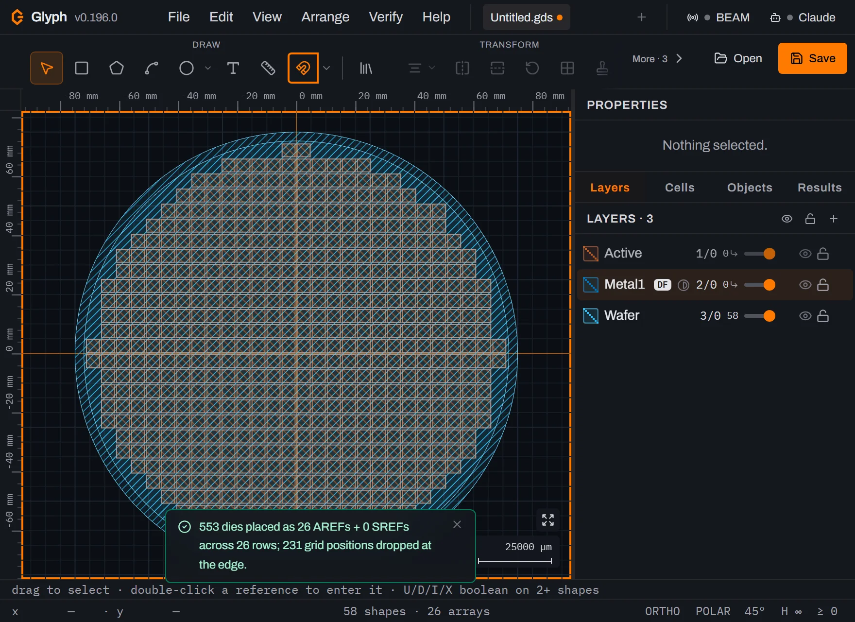 View full image
Look at where dies get dropped. Zoom to the bottom of the wafer, where the primary flat and the edge exclusion both cut into the die grid. Whole rows of the rectangular candidate grid simply aren't drawn there — the planner never emits a die whose footprint would cross the flat or fall inside the exclusion band, so "dropped" isn't a visual gap you have to clean up, it's positions that were never placed.
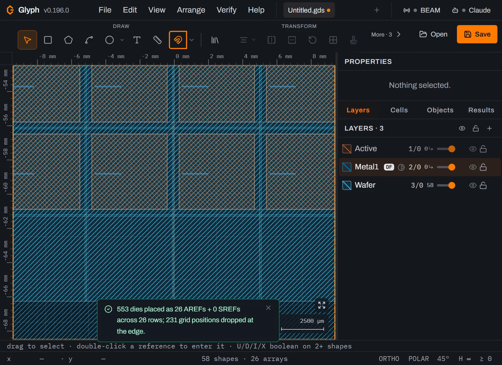 View full image
Set up an alignment-mark set. Choose . Leave MARK TYPE on its default, Alignment cross (+) — a classic photolithography cross, 100 µm tip to tip with 20 µm arms. The POSITIONS (µm) box wants one
x, ypair per line, which is exactly what its own first line says:# x, y in µm — one mark position per line. Keep that comment line, delete the0, 0under it, and type three positions:-40850, -40850 40750, -40850 -50, 45850Those numbers look arbitrary and aren't. Marks belong in the dicing streets, not on a die, and with DIE ORIGIN on lower-left the die footprints run
[5100·i, 5100·i + 5000]µm on both axes — so the street between two columns is 100 µm wide (pitch 5100 minus die 5000) and centred on5100·i + 5050µm. Each coordinate above is a street crossing, and the 100 µm cross therefore spans its street exactly, end to end. Finally, make sure both1/0 — ACTIVEand2/0 — METAL1are ticked under LAYERS — the dialog pre-ticks whichever layer is current, which isMetal1(current since step 6), so1/0 — ACTIVEis the one you tick yourself — and leave3/0 — WAFERalone. The summary line reads3 position(s) × 2 layer(s) = 6 marks, one undo entry., and because Metal1 is dark field the dialog warns that the mark is emitted there as a window — the cross knocked out of a clear surround — instead of solid geometry, so the same mark prints as the same image on a clear- and a dark-field level.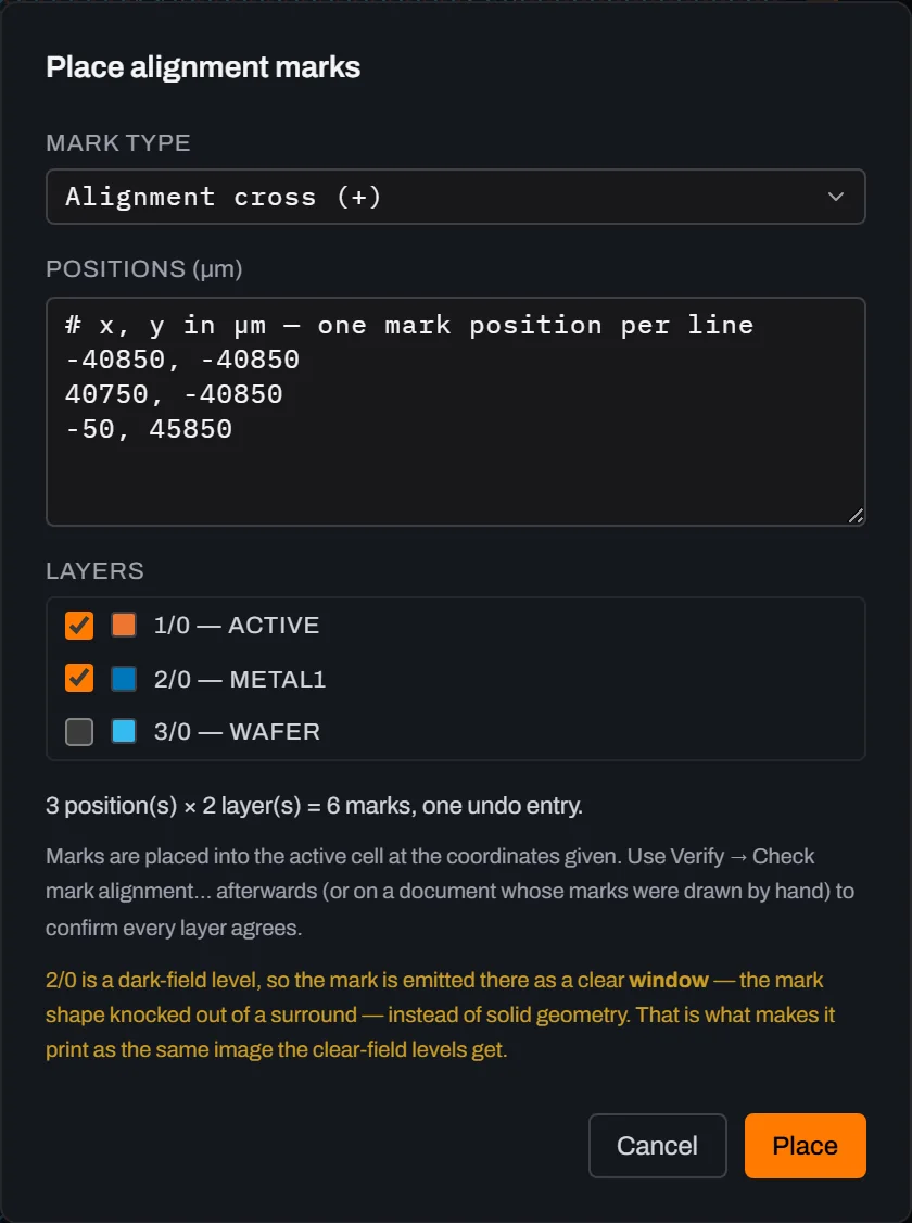 View full image
Place the set and look at one mark. Click Place. Nine shapes land in
TOPin one undo entry — six on the clear-field layer (two boxes per cross, three crosses) and three on the dark-field layer (one windowed polygon per cross) — and the toast readsPlaced 6 marks (9 shapes) on 2 layers.The status bar reads67 shapes · 26 arrays. Now navigate to the first position,-40850, -40850µm — and use the live cursor read-out at the bottom-left of the status bar (x … · y …) as your compass: zoom toward the wafer's lower-left quadrant, watching the read-out approach those numbers; the mark sits on the street crossing nearest the flat's left end. The dicing lanes sit directly under the mark there, which is the point of putting it in a street but makes for a busy picture, so click the eye button on the Wafer row in the Layers tab to hide them; it becomes a crossed-out eye and that row's 58 shapes stop drawing. What is left is the mark, on both levels at once: the orange cross is the mark on Active, the clear-field level, and the blue hatched square around it is Metal1's dark-field window with a cross-shaped hole knocked out of it — both centred on the same coordinate, because they came from the same(x, y)in the same placement. The hairline running from the square's corner to the hole is the seam where that polygon closes; GDS boundaries have no hole primitive, so a hole is cut with a keyhole slit.Click either arm of the cross to check the size claim for yourself: the status bar picks up
· 1 selected, the Properties panel reads W100.00 µm, H20.00 µmon layerActive (1/0), and the inline badges on the canvas say the same. That is the 100 µm cross, exactly as long as the street is wide.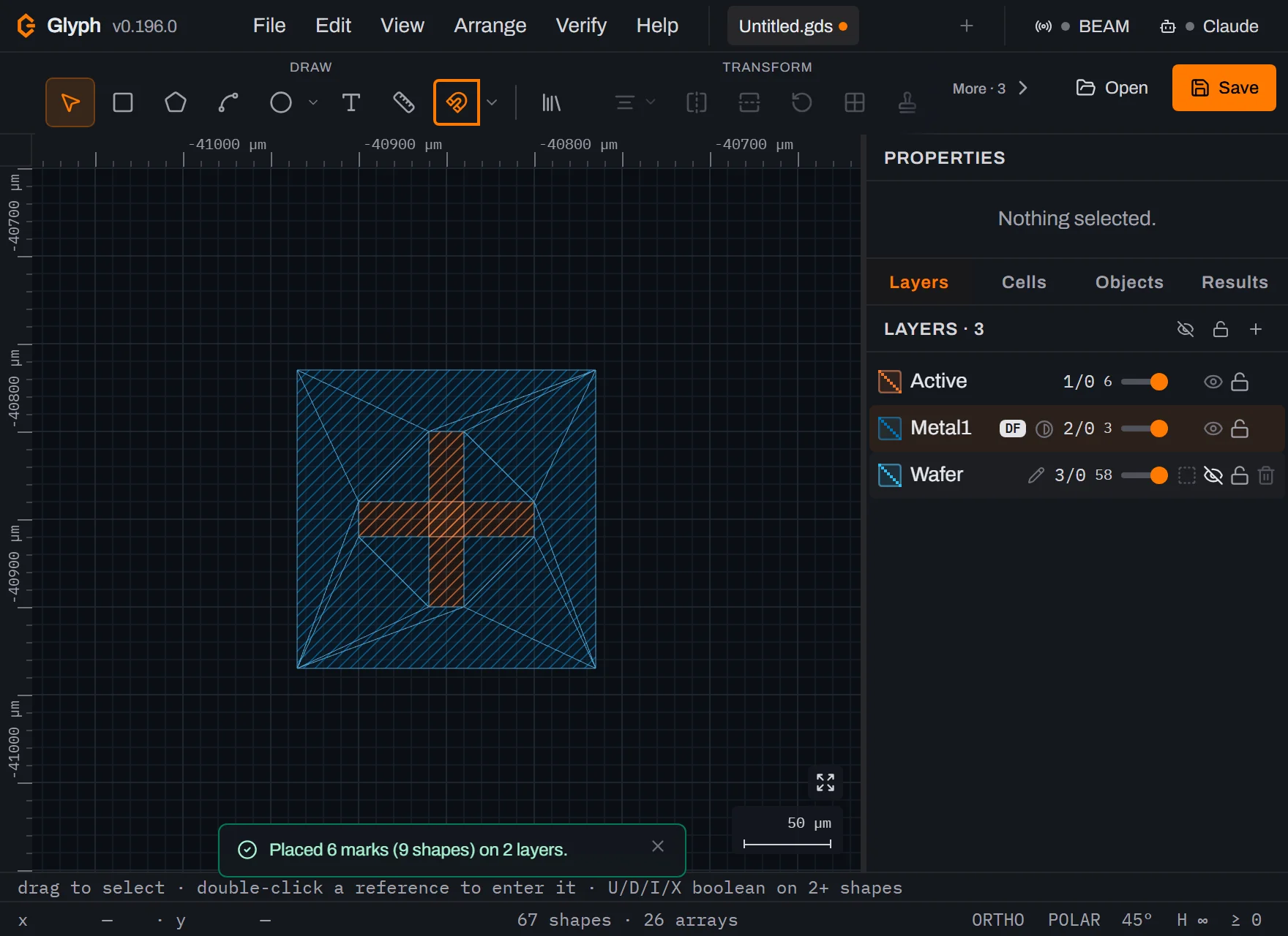 View full image
Cross-check every level. Choose . This is read-only — it dispatches no command and touches nothing on the canvas. It expands every SREF/AREF instance in
TOPfirst (so a mark buried inside a referenced cell on one level and drawn directly on another would still be compared), clusters small shapes per layer into candidate marks, then matches marks across layers within a tolerance. The report:Layers carrying mark-like shapes: 1/0, 2/0,Mark sites found: 3, andAll 3 mark sites agree across every layer. No action needed.The 553 dies' own geometry never shows up as a false mark: the 4400 µm active square and the 1500 µm trace are both past the check's ownmax mark size 500 µmcutoff, which is stated in the report header beside the tolerance and the two cluster radii.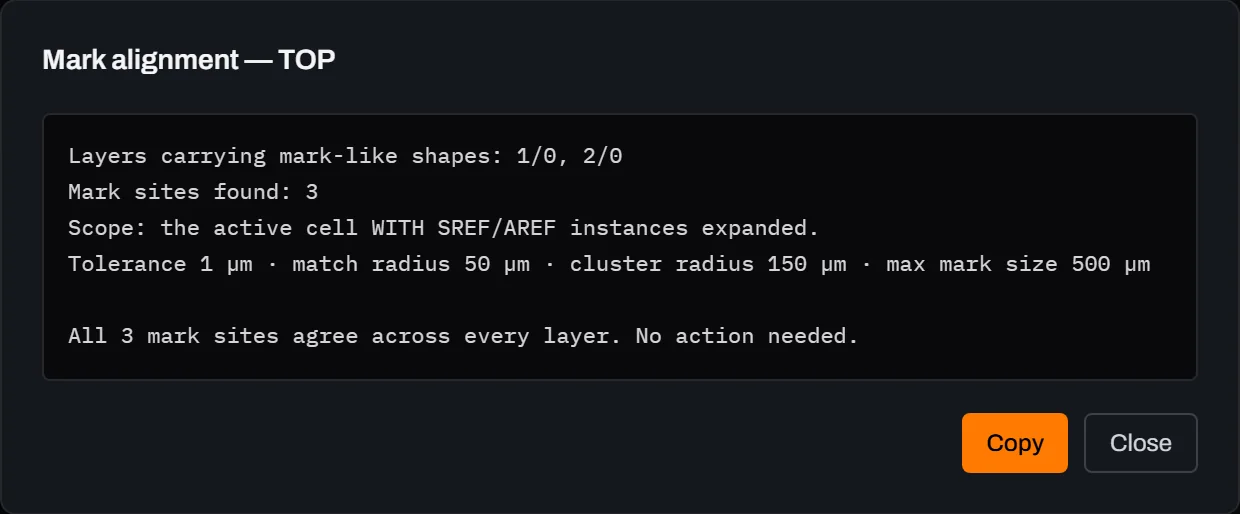 View full image
Placing dies from a stepper job file (CSV)
above computes a uniform grid — every die at the same pitch, on a regular lattice. Real stepper jobs aren't always that clean: a job file from an aligner, a list of known-good sites from a prior wafer map, or a job that mixes two die types at different positions all need dies placed at specific, possibly irregular coordinates instead of a computed grid. is built for exactly that — read a coordinate file, place one SREF of a chosen cell at every row, with a full preview before anything commits.
The file format mirrors the CSV review-marker importer you'd already know from a DRC or .lyrdb
workflow (§3): comma or tab delimited, a header row detected and skipped automatically, #
comments and blank lines ignored. Recognised columns, in this fixed order, are x, y (the only two
required), then rotation, magnification, reflect, cell — all four optional. Try it against
the DIE cell you already built, well clear of the wafer field so it's easy to spot — this is a
standalone example, not a continuation of the wafer scene above:
x, y, rotation
120000, 0, 0
140000, 0, 90
160000, 0, 180
Open the dialog, click Choose CSV file… and pick that file (or paste it into a .csv first),
set Coordinate unit to µm to match the numbers above, and set Cell to place to DIE. The
summary line reads 3 valid rows — no refusals, because every row parses and none of the checks
below caught anything. Click Place, and three SREFs of DIE land at those coordinates, well
off to the side of the wafer you generated, each carrying its row's rotation, in one undo step
for the whole file regardless of row count.
Two details worth knowing before you point this at a real job file:
- The
cellcolumn overrides the dialog's chosen cell for that one row only — the workflow a mixed-die-type job needs, without splitting the file in two. A row naming a cell that doesn't exist, that would place a cell into itself, or that would create a reference cycle is refused and counted rather than silently skipped, alongside a malformedx/y/rotation/magnification/reflectvalue — the dialog's preview lists every refusal with its line number and reason before you commit anything. - The same 2,000-copy cap Polar array uses applies here. A file asking for more is refused outright, naming both the requested count and the limit, so a job file with tens of thousands of sites needs splitting (or a different tool) rather than silently placing a truncated subset.
What you built
A 5 mm die drawn from a blank document — two layers, named and toned, a 4.4 mm active area and a metal trace, sized by typing rather than by dragging — then stepped into 553 copies across a 150 mm wafer as 26 AREFs and zero SREFs, in one undo entry, with dicing lanes derived straight from the 5.1 mm pitch and dies dropped wherever the primary flat or the 3 mm edge exclusion would clip them. On top of that, a three-site alignment-mark set in the scribe streets spanning a clear-field and a dark-field layer, placed in one more undo entry and confirmed, by a read-only geometric check, to agree at every site to within 1 µm. Close the report, un-hide the Wafer row and press Ctrl+0 to see all of it at once — at full-wafer scale the 100 µm marks are far below one pixel, which is the honest reason you cannot see them there.
Next steps
Read Arrange for the rest of the alignment, distribution and array toolkit that Wafer layout sits alongside, and Layers for how mask field tone (clear vs. dark) works and why it changes how a mark gets drawn. Design rule checking covers Glyph's other read-only Verify-menu check, run the same way as the mark-alignment report here. Then open the editor and step your own die across a wafer.